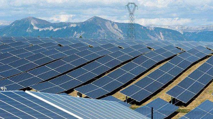
Applications of CO2 Lasers in the Photovoltaic Cell Industry
Laser technology serves as an effective means for reducing costs and enhancing efficiency in the photovoltaic cell industry. It demonstrates significant advantages over traditional methods in various processes, including etching, grooving, doping, repairing, and metallization. The application of laser technology presents vast potential for development across different battery technologies, paving the way for further innovations and improvements in solar energy production.
1. Applications of Laser Technology in PERC Cells:
Laser technology plays a crucial role in the PERC cell sector, encompassing processes such as laser doping (Selective Emitter, SE), laser ablation, and laser scribing. Laser ablation and doping have become standard techniques, while other niche applications include laser MWT (Metal Wrap Through) drilling and LID/R (Light-Induced Degradation/Repair).
- Laser Doping Equipment: Selective Emitter (SE) utilizes the selective heating characteristics of lasers to create a high-concentration phosphorus-doped n++ region at the junction between the electrode grid and the silicon wafer, based on the phosphorus-silicon glass layer formed during the diffusion step. This process enhances the doping concentration in the electrode contact area, thereby reducing contact resistance.
- Laser Ablation Equipment: This technology precisely etches the passivation layer using lasers to achieve micro-nano-level high-precision local contacts. It is one of the core processes enhancing the passivation in PERC technology, necessitating precise energy distribution, control of action time, and pulse stability. With PERC technology, the photoelectric conversion efficiency of monocrystalline cells can be improved from 20.3% to 21.5%.
- Other Equipment: a) MWT Drilling Equipment: Utilizing metal perforation wrapping technology for laser drilling, this method directs the current collected by the front electrode through the openings filled with silver paste to the back side, eliminating the main grid lines on the front to reduce shading. Due to its niche application, the MWT equipment is limited to a few companies, such as Daystar Photovoltaics. b) LID/R Repair Equipment: Employs ultra-high power lasers to irradiate the cell, reducing carrier recombination losses and thereby minimizing light-induced degradation. Common methods for reducing light-induced degradation include thermal treatment and halogen lamp irradiation, which can be integrated with the sintering process. Consequently, laser repair is currently less common in P-type cells. C) Laser Scribing Equipment: Used for cutting half-cells and bifacial modules, this includes thermal laser cutting and non-destructive laser cutting techniques.
2. Applications of Laser Technology in N-Type Cells:
The use of laser technology in N-type cells encompasses laser doping, laser repair, laser etching, and laser transfer, with the potential for value growth expected to multiply compared to the PERC era. Consequently, the ramp-up of N-type cell production will significantly expand the market for photovoltaic laser equipment.
TOPCon: Laser doping enhances efficiency and is anticipated to become a standard process.
In the production process of TOPCon cells, laser technology can be utilized in selective re-doping (SE process) and laser transfer applications.
HJT: Laser repair can reliably maintain efficiency gains.
Heterojunction (HJT) is a unique PN junction formed by the deposition of amorphous silicon onto crystalline silicon, classified as a type of N-type cell. The application of light in HJT cells includes laser repair for LIR and laser transfer.
IBC: Laser grooving effectively addresses challenges in IBC cell fabrication.
IBC cells can be combined with various technologies, including HJT, TOPCon, and perovskite, to unlock significant efficiency potential. The key processes for IBC cells involve creating interdigitated P and N regions, developing superior surface passivation layers, and metallization.
Currently, laser grooving technology is primarily applied in 1) IBC cells for Etching masks and fabricating cross-finger structures in the PN junction; 2) PN region isolation; 3) Passivation layer grooving.
Laser grooving allows for the cost-effective fabrication of PN junction structures. A critical issue in IBC cell processes is the creation of spaced interdigitated P and N regions, along with achieving optimal surface passivation and metallization. This addresses current challenges in IBC technology, such as the need for multiple masking steps, which complicate the process, and the risk of leakage between PN electrodes. By utilizing laser etching, the masking step can be bypassed, enabling more cost-effective PN region fabrication and allowing for flexible and precise removal of passivation layers to form metallized contact areas.
Furthermore, laser grooving can be applied for isolating the PN regions in IBC cells. To prevent short circuits, isolation between the P and N regions at the back of the XBC cell is often necessary. Various methods for PN region isolation exist, including the use of undoped amorphous silicon to prevent direct communication between P-type and N-type doped areas, or applying laser grooving between these regions for effective isolation.
Additionally, laser grooving can be implemented in the etching of contact structures after the formation of the passivation layer and before the onset of metallization in IBC and TBC cells. The purpose of laser grooving the passivation layer is to open windows on the back of the N-type monocrystalline silicon wafer, allowing electrodes to be connected from the N and P regions for metallization. The back passivation layer in back-passivated cells typically consists of aluminum oxide and silicon nitride, aluminum oxide and silicon oxide, or doped polycrystalline silicon and silicon oxide. The thickness of the aluminum oxide generally ranges from 5 to 20 nm, while silicon nitride ranges from 70 to 220 nm. Commonly, the aluminum oxide thickness is around 10 nm, with silicon nitride between 70 and 100 nm, resulting in a light blue appearance for the back passivation layer; some manufacturers enhance the surface passivation effect by incorporating polishing processes, achieving a higher light reflectivity in the visible spectrum compared to other wavelengths.
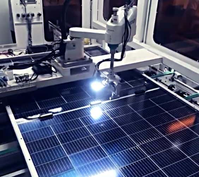 3. Laser Transfer: A Versatile Metallization Technology with Significant Cost Reduction Potential
Laser transfer is an innovative non-contact metallization technique applicable to all types of solar cells, including PERC, TOPCon, HJT, and IBC. Electrode metallization is a critical process for fabricating solar cell electrodes and is essential in photovoltaic cell manufacturing. While various methods exist for electrode metallization, the current mainstream approach is contact-based screen printing. The industry is actively exploring the industrialization of new metallization methods, such as laser transfer and copper plating, to further reduce costs and enhance efficiency in solar cell production.
Laser transfer presents significant advantages over screen printing and is poised to become one of the leading technologies. The primary benefits of laser transfer compared to traditional screen printing include:
- Finer grid lines: Laser transfer can achieve grid line widths below 18 microns, leading to a 30% reduction in paste usage. This efficiency has already been validated in PERC cells, with even greater savings expected in TOPCon and HJT processes.
- Excellent consistency and uniformity: The printing height is remarkably consistent, with a variation of only 2 microns, and is compatible with low-temperature silver paste.
- Customizable groove shapes: The groove design of the flexible membrane can be adjusted to suit different cell structures, optimizing grid line configurations and enhancing electrical performance.
- Non-contact printing: Laser transfer avoids issues associated with contact printing, such as micro-cracking, chipping, contamination, and scratching. As the trend toward thinner wafers continues, the risk of micro-cracking increases; however, the non-contact nature of laser transfer effectively addresses this problem.
Laser transfer is a universal technology with vast potential for future industrialization. It is applicable to all photovoltaic cell metallization processes without bias towards specific cell technologies or paste types, including PERC, TOPCon, HJT, and IBC. It accommodates various paste types, such as high-temperature silver paste, low-temperature silver paste, and silver-coated copper paste. Given that N-type cells like TOPCon and HJT utilize double-sided silver paste and that the low-temperature silver paste used in HJT has higher viscosity and silver consumption, the cost of silver paste for these cells is currently significantly higher than that for PERC cells. The adoption of laser transfer can effectively reduce the silver paste costs associated with N-type cells, thereby accelerating their industrialization process.
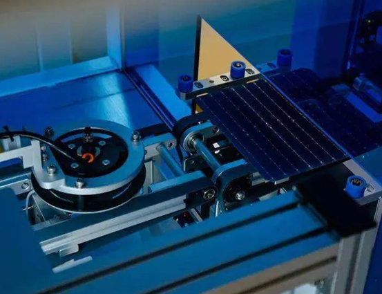
4. Applications of Laser Technology in Modules: Thin Film Perforation and Non-Destructive Cutting/Slicing
Laser Thin Film Perforation: This technique is used for perforating double-glass solar modules. Both the front and back panels of double-glass modules require photovoltaic glass, and the back glass must be perforated at specific locations to allow the current leads of the solar cell module to be routed to the junction box. Thus, perforating the back glass is an essential step in module processing.
Currently, there are two methods for drilling holes in the back glass of double-glass modules: mechanical and laser methods. Compared to traditional mechanical methods, laser drilling offers the following advantages:
- The initial fixed investment for laser technology is high; however, it incurs lower maintenance costs over time. This is attributable to the mechanical method's need for the replacement of consumable glass drill bits, as well as the requirement for cooling water spray and collection systems.
- Laser drilling allows for the seamless transition between various hole shapes and diameters, including round, square, and custom forms.
- The processing yield is exceptionally high. Based on practical data from HAN’S LASER, the drilling yield for 2.5 mm thick glass using laser methods is approximately 5% greater than that of mechanical drilling. As the trend towards thinner and lighter photovoltaic glass progresses, the advantages of laser processing in yield are anticipated to become even more significant.
- The precision and quality of the processing are exceptional, resulting in clean hole walls free from dust residue and minimal damage.
Laser Non-Destructive Cutting: This technique replaces traditional cutting methods that cause damage, resulting in no micro-cracking and lower thermal damage. It reduces efficiency loss in modules by 0.05 and is compatible with various mainstream cell types, including PERC, TOPCon, and HJT. Conventional slicing of half-cells or shingled cells employs laser thermal cutting, which forms molten grooves on the cell surface using a focused laser beam, followed by the application of an external breaking force. This method can produce micro-cracking at the cut surface and create significant thermal effects on the cell surface, potentially leading to greater efficiency losses in thinner HJT cells.
In contrast, non-destructive cutting technology can utilize separated laser irradiation or an off-axis light path to induce cracks in the solar cells that propagate and separate without causing hidden cracks. This method is expected to reduce efficiency losses at the module level by 0.05 while also contributing to improved production yields.